Pages

Wind-Solar Hybrid Power Model

Wind power generation and solar power generation are combined to make a WIND-SOLAR HYBRID POWER GENERATION SYSTEM. A 6v, 5Ah lead-acid battery is used to store solar power and charging is controlled by a charger circuit.

Design Estimation of 5KWp BIPV Solar Power System

Design Estimation of 5KWp BIPV Solar Power System

Intenet access through LED Bulb

A new emerging technology for internet and data sharing. data can be sent and recieved at speed of 100gbps.

Hydrogen Fuel Cell !!! New source of 'R'energy

This is the world’s first scalable Hydrogen-On-Demand process requiring minimum power input

Download Free Android App For REnergy!!

This is a free android app for this blog : REnergy. I've built this app for the users of my blog to access my posts, works with ease.

Tuesday 30 April 2013

Solar Inverter : Classification

The solar inverter is a critical component in a solar energy system. It performs the conversion of the variable DC output of the Photovoltaic (PV) module(s) into a clean sinusoidal 50- or 60 Hz AC current that is then applied directly to the commercial electrical grid or to a local, off-grid electrical network. Typically, communications capability is included so users can monitor the inverter and report on power and operating conditions, provide firmware updates and control the inverter grid connection. Depending on the grid infrastructure wired (RS-485, CAN, Power Line Communication, Ethernet) or wireless (Bluetooth, ZigBee/IEEE802.15.4, 6loWPAN) networking options can be used. To know more about solar inverter please view the post.


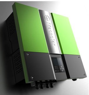
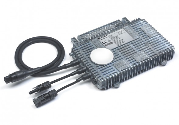
Function Of a Solar Inverter


A solar inverter, or PV inverter, converts the
variable direct current (DC) output of a photovoltaic
(PV) solar panel into a utility frequency alternating
current (AC) that can be fed into a commercial
electrical grid or used by a local, off-grid electrical
network. It is a critical component in a photovoltaic
system, allowing the use of ordinary commercial
appliances. Solar inverters have special f unctions
adapted f or use with photovoltaic arrays, including
maximum power point tracking and anti-islanding
protection.


A little More About Solar Inverters

The engineering of these solar inverters and solar panels are designed like pieces of puzzles which should fit together in order to function. Conclusively, these solar inverters are programmed to hook up to a specific count of solar boards. The cost of inverter is practically 10 percent of the total cost of the solar board. We have to take note that these solar inverters do not have useful lives equally long as that of solar panels. This means you have to replace your solar inverters from time to time for you to use your solar system for its remaining useful life. For a solar inverter to work efficiently it should have adequate solar panels connected to it. Lesser or more panels that are connected to it could cause it not to function properly. Consequently, it should have at least 95 percent of panels hooked up to obtain optimum performance.


Classification

Solar Inverter can be classified into 4 major type.They are:

  1. Stand-alone inverters 

used in isolated systems where the inverter draws its DC energy f rom batteries charged by photovoltaic arrays. Many stand-alone inverters also incorporate integral battery chargers to replenish the battery f rom an AC source, when available. Normally these do not interf ace in any way with the utility grid, and as such, are not required to have anti-islanding protection.


  2.  Grid-Tie Inverters

This type of inverters match phase with a utilitysupplied sine wave. Grid-tie inverters are designed to shut down automatically upon loss of utility supply, f or safety reasons. They do not provide backup power during utility outages.


3.   Battery Backup Inverters

Thsese are special inverters which are designed to draw energy from a battery, manage the battery charge via an onboard charger, and export excess energy to the utility grid. These inverters are capable of supplying AC energy to selected loads during a utility outage, and are required to have anti-islanding protection.


4.   Micro-Solar Inverter

Solar micro-inverters convert direct current (DC) from a single solar panel to alternating current (AC). The electric power f rom several micro-inverters is combined and sent to the consuming devices. The key feature of a micro-inverter is not its small size or power rating, but its one-to-one control over a single panel and its mounting on the panel or near it which allows it to isolate and tune the output of that panel.
these micro inverters are most suitable for domestic-solar PV-application where the no. of solar panels are limited to few. Detail about the Micro-solar inverter will be cited in another post.


Here is Heirarchy Model of Solar Inverter Classification


Follow me on Academia.edu
About the Author

Amrit Mandal is a final year B.tech (EE) Student, Admin of this blog. He likes to work in the renewable energy field-specially in solar energy field.
Follow Us on Twitter #REnergy_Blog

REnergy

Monday 29 April 2013

LITER OF LIGHT


We dream about tomorrow’s glowing world………...........We are the team of “Liter of Light” in India……..
Mission
spreading this innovation in our country and installing the liter of light in India.
Description
The  source of light consists of a plastic bottle filled with a water solution which is embedded in the roofs of houses. The solar bottle harnesses the light from the sun, capturing and diffracting the light to all parts of the room. Our aim is to support this idea which has already launched in many countries around the world.
 Founded - September 12,2011
Products- A soda bottle as a light source in underprivileged households.


Liter of Light India Abstract :
             We are a group of under graduate students working to install liter of lights or solar blubs all over India.Our motto is to lighten up the most unprivileged communities by installing solar bulbs.Introducing such low-cost technologies we aim to glow about one million homes throughout India.
What is Liter of Light :
              A Liter of Light is a zero-carbon emitting solar lighting project which is first initiated by members of My Shelter Foundation and students of the Massachusetts Institute of Technology.Solar Bottle Bulb uses appropriate technologies that are highly replicable and sustainable. The materials used are found easily in the poorest neighborhood.They can be easily built with simple carpentry skills and little knowledge about the solar bulb. This simple mechanism of installing Solar Bottle Bulb made the expansion of movement easy.
Do it Yourself Liter of Light:
               The bulb is nothing but a A 1.5 liter clear PET bottle which is used as source of light.It is filled with the mixture of water and bleach.The bottle with this mixture is inserted into a metal sheet.This kit is embedded on the roofs of houses which acts as a source of light.
Working principle of Liter of Light :
                Solar Bottle Bulb works by the refraction of light rays.The sun rays falling on the bottle gets refracted when it immediately enters water i.e. due to change in medium form air to water.This refracted light spreads at an angle of 360 degrees in a room and produces light equivalent to 60 watts bulb.
                The solar bulb lasts for 5 years without any sort of maintenance with the change of water at regular intervals.Bleach is added to maintain the clarity of water and make the water free from microorganisms.
 Why Liter of Light :

  • Solar Bottle Bulb does not have any carbon emissions when compared to any conventional light.
  • Solar Bottle Bulb is a source of livelihood for the local unemployed people.
  • It is very economic and reliable.
  • It reduces the impact of global warming on earth.
  • Disposed plastic is up-cycled.
      https://www.facebook.com/pages/Liter-of-Light-in-India/204926342960861 - FOLLOW THIS LINK .

FPGA vs ASIC

FPGA --- Field-Programmable Gate Array
ASIC --- Application-Specified Integrated Circuit
A field-programmable gate array (FPGA) can be purchased off-the-shelf and programmed by the user, whereas an application-specific integrated circuit (ASIC) is manufactured to a customer’s specification. This distinction has not changed since the dawn of both technologies.


Time-to-market and configurability
The configurability of an FPGA is its most priced asset. Its ability to rapidly implement or reprogram the logic for a specific feature, or to modify the functionality that was previously instilled in it, is why designers run after it.


“Even if a vendor has new features to add at a later stage in the released product, he still has the freedom to decide whether to implement that feature in software or hardware based on applicability. Time-to-market for handling change-requests in FPGA is much less than in ASICs,” explains Manisha Mankar, architect—digital design, Robert Bosch Engineering and Business Solutions.

Indeed, this is one of the primary reasons why designers are opting for FPGAs.

“There are two key factors driving the demand for FPGAs today: The programmable imperative, i.e., the inherent capability of an FPGA that allows it to be tailored to the needs of the customer and the insatiable bandwidth requirements of the mobile generation today. Given this, FPGAs are increasingly replacing ASICs and ASSPs for more and more applications across different verticals such as telecommunications, aerospace, medical, automotive and industrial to name a few,” adds Neeraj Varma, director-sales, Xilinx India.


 Performance and power efficiency
While FPGAs used to be selected for lower-speed, less complex or volume designs in the past, today’s FPGAs easily push the performance barrier. With increase in logic density and other features such as embedded processors, DSP blocks and high-speed serial at low price points, FPGAs are an interesting proposition. The industry has shown that high-end FPGAs are growing in volume, handling high-speed applications and complex designs.Earlier, FPGAs were viable only for prototyping or low-density applications. Now they meet the needs of very high-volume applications such as consumer products and other moderate-volume high-density appli-cations as well.
The fact that ASICs are built for specific applications allows them to have a very high density of useful logic gates on the chip and use resources optimally. Hence higher gate count and lower power consumption give ASICs a competitive edge over FPGAs. 

High volume production

For high-volume production, costs associated with building a custom ASIC chip are said to be increasing, especially since technology nowadays is ever more complex. As we move towards advanced nodes, cost considerations multiply exponentially. For instance, the development cost for ASIC at 28nm is 40 per cent more than at 40nm. At 20nm, it is estimated to be 70 per cent over that of 28nm.

Best of both the worlds
While FPGAs are excellent for designing and prototyping digital logic into medium-volume, medium-density applications, their high unit cost makes things difficult. On the other hand, the low unit cost of ASICs is one of the main reasons why these are considered for high-volume manufacturing.

What if there were a way to get the best of both the worlds? Well, designing a new product around FPGA allows design modifications to be quickly made throughout the development process. Once this design is complete and approved for production, the FPGA design can be migrated to an ASIC design and then produced, cutting the production unit cost greatly.


Sunday 28 April 2013

LEDs for Solid-state Lighting

Solid-state electronics has been transforming our lives for many decades by bringing us increasingly small, cheap and efficient devices and appliances. Our modern life-styles have come to be defined by our access to an increasingly wide assortment of technologically advanced equipment for personal and group use. From smart phones to personal music players and from satellite navigators to tablet computers the benefits of modern electronics are all around us. In this continuing tradition, solid-state lighting now seems set to revolutionise the way we light our surroundings - indoors and outdoors. Its impact is already being felt globally and in the coming years it will further entrench its position as one of the defining technologies of the twenty-first century. 


Lighting technology has changed remarkably little since its inception more than a hundred years ago. We still illuminate our homes and offices with lamps that bear a striking resemblance to Thomas Edison’s invention in the late nineteenth century. Indeed the basic design of incandescent light bulbs has remained essentially the same over the years and with that their efficiencies have also changed very little. The development of tungsten-halogen lamps in the nineteen-fifties did raise the efficiency somewhat but it still remained woefully low. The later development of fluorescent lighting resulted in a big improvement in efficiency but even that is now considered insufficient in our increasingly energy-conscious world. Moreover, their use of toxic and environmentally hazardous mercury has always remained a cause for concern. The emergence of highly efficient diode-based solid-state lighting over the past decade has, therefore, been widely welcomed and acknowledged as the next logical step in the evolution of lighting technology.

Solid-state light emitters were invented in the nineteen sixties as semiconductor pn-junction diodes capable of emitting coloured light. These light-emitting diodes (LEDs) were made from materials such as gallium arsenide and gallium arsenide phosphide. For many years, LEDs only served as small indicator lights for electronic equipment. They were ubiquitous in everything from portable transistor radios to televisions and telephones. Epoxy-packaged low-power LEDs are still around in essentially the same form in which these devices have been used for several decades.  In later years, LEDs were also used to build dot-matrix displays that found particular favour in countries of the far-east. Even today a visitor to such places as Hong Kong, Singapore or Tokyo cannot escape the overwhelming concentration of advertising LED bill boards in city centres. Traffic light is another application where LEDs made an early appearance.

A typical LED-based traffic light utilising clusters of low-power red, amber and green LEDs is shown in figure.

LEDs were traditionally available in most colours except blue which made it impossible to build full-colour displays using a combination of red, green and blue light emitters. A blue-emitting LED was a long sought after goal and, therefore, it caused much excitement when a practical blue LED was reported by a researcher at a small Japanese electronics company. Following figure  shows an LED wafer with many individual blue LEDs, undergoing testing on an assembly line. Shuji Nakamura’s invention of the blue LED at Nichia Corporation resulted in the proliferation of LEDs in all kinds of applications. Its development also gave rise to the white LED which consists of a blue LED chip coated with a light-emitting material called a phosphor. The phosphor gets excited by the blue light from the LED chip and converts a large amount of the blue light into yellow light. The resulting light – a combination of yellow emission from the phosphor and the residual un-converted blue light – appears white to our eyes. The availability of white LEDs soon started people thinking about the possibility of using these devices for illumination purposes.
 
 Early LEDs were low-power devices, capable of running at no more than a quarter of a watt of power dissipation. While this was adequate for use as indicator devices and even for multi-colour dot-matrix displays, space lighting demanded higher power devices. This was a formidable problem once because high power LEDs have to use larger chips that also produce much more heat than the tiny chips used in conventional low-power LEDs. It took several years for device packaging technology to advance to the point where half watt LEDs could become commercially available. Companies such as Philips and General Electric spearheaded these developments, resulting in the eventual availability of watt-class white LEDs. Once these devices became available, systems designers set thinking about designing lighting systems that could take advantage of the many benefits offered by LED-based luminaires.

A radical departure from conventional means of generating light, LEDs have features that make them especially suited for lighting applications. Their small size, extreme efficiency in converting electrical energy to light, availability in many colours (including white) and absence of any environmentally harmful substance that might pose a problem during disposal make them ideal as light sources for any conceivable application. Little wonder then that LED-containing lighting systems are finding increasing acceptance all over the world. The market for LEDs and solid-state lighting systems has been growing at close to 25% per annum for the past several years and by all indications will continue to do so for the foreseeable future.

 The first luminaires to be designed with high power white LEDs were shaped to resemble traditional tungsten filament light bulbs. These so-called retrofit bulbs have standard screw or bayonet bases to fit in existing lamp sockets. The argument was that this was the quickest way to market for LED lamp makers as it required no modification of existing lighting infrastructure. In spite of their significantly higher cost, the sales of retrofit LED light bulbs have been rising over the past five years. Manufacturers cite their very long lifetimes as the feature that offsets their purchase price – a typical LED light bulb can last for 10,000 to 20,000 hours before needing replacement. Compare this with the typical 800 hours lifetime of a tungsten incandescent bulb and the higher cost of an LED bulb doesn’t seem too onerous. The increased cost of these bulbs results from the need to incorporate a complete power supply inside every bulb, as LEDs only operate with low voltage DC power. The power supply is also the most vulnerable part of any LED bulb because the failure of any of its components can render the bulb useless. The actual LEDs themselves are much less prone to failure and are the reason manufacturers are able to quote such ambitious figures for their products.Above figure 3 shows the interior of an 8 watt bulb containing 6 surface mount power LEDs. With prolonged use, LEDs tend to grow dimmer and a bulb’s useful life is considered over once its LEDs drop to half of their initial brightness. The fall in brightness is caused by a slow degradation of the LED chip and the colour conversion phosphor. The fact that LED bulbs do not fail abruptly like incandescent bulbs also reduces chances of untoward accidents.
                                                      A 12 Watt LED bulb from Philips

Saturday 27 April 2013

Future wire ''NANOWIRE''

A nanowire is a nanostructure, with the diameter of the order of a nanometer (10−9 meters). Alternatively, nanowires can be defined as structures that have a thickness or diameter constrained to tens of nanometers or less and an unconstrained length. At these scales, quantum mechanical effects are important — which coined the term "quantum wires".

Many different types of nanowires exist, including metallic (e.g., Ni, Pt, Au), semiconducting (e.g., Si, InP, GaN, etc.), and insulating (e.g., SiO2, TiO2). Molecular nanowires are composed of repeating molecular units either organic (e.g. DNA) or inorganic (e.g. Mo6S9-xIx).

The nanowires could be used, in the near future, to link tiny components into extremely small circuits. Using nanotechnology, such components could be created out of chemical compounds.

Synthesis of nanowires

There are two basic approaches to synthesizing nanowires: top-down and bottom-up. A top-down approach reduces a large piece of material to small pieces, by various means such as lithography or electrophoresis. A bottom-up approach synthesizes the nanowire by combining constituent adatoms. Most synthesis techniques use a bottom-up approach.
Nanowire production uses several common laboratory techniques, including suspension, electrochemical deposition, vapor deposition, and VLS growth. Ion track technology enables growing homogeneous and segmented nanowires down to 8 nm diameter.

Suspension

A suspended nanowire is a wire produced in a high-vacuum chamber held at the longitudinal extremities. Suspended nanowires can be produced by:
  • The chemical etching of a larger wire
  • The bombardment of a larger wire, typically with highly energetic ions
  • Indenting the tip of a STM in the surface of a metal near its melting point, and then retracting it

VLS Growth

A common technique for creating a nanowire is Vapor-Liquid-Solid (VLS) synthesis. This process can produce crystalline nanowires of some semiconductor materials. It uses as source material either laser ablated particles or a feed gas such as silane.
VLS synthesis requires a catalyst. For nanowires, the best catalysts are liquid metal (such as gold) nanoclusters, which can either be self-assembled from a thin film by dewetting, or purchased in colloidal form and deposited on a substrate.
The source enters these nanoclusters and begins to saturate them. On reaching supersaturation, the source solidifies and grows outward from the nanocluster. Simply turning off the source can adjust the final length of the nanowire. Switching sources while still in the growth phase can create compound nanowires with super-lattices of alternating materials.
A single-step vapour phase reaction at elevated temperature synthesises inorganic nanowires such as Mo6S9-xIx. From another point of view, such nanowires are cluster polymers.

Uses of nanowires

Nanowires still belong to the experimental world of laboratories. However, they may complement or replace carbon nanotubes in some applications. Some early experiments have shown how they can be used to build the next generation of computing devices.
To create active electronic elements, the first key step was to chemically dope a semiconductor nanowire. This has already been done to individual nanowires to create p-type and n-type semiconductors.

The Future 

The next step was to find a way to create a p-n junction, one of the simplest electronic devices.

After p-n junctions were built with nanowires, the next logical step was to build logic gates. By connecting several p-n junctions together, researchers have been able to create the basis of all logic circuits: the AND, OR, and NOT gates have all been built from semiconductor nanowire crossings.


Follow me on Academia.edu
About the Author

Amrit Mandal is a final year B.tech (EE) Student, Admin of this blog. He likes to work in the renewable energy field-specially in solar energy field.
Follow Us on Twitter #REnergy_Blog

REnergy

Friday 26 April 2013

Sensitive Smart Skin : New Technology

An array of piezotronic transistors capable of converting
mechanical motion directly into electronic controlling signals
Knitting  zinc oxide nano-wires vertically, researchers of Georgia Institute of Technology have fabricated arrays of piezoelectric transistors which are capable of converting mechanical motion directly into electronic controlling signals.It can sense touch with the same level of sensitivity as the human fingertip, which could result in better bots and prosthetic.


"Any mechanical motion, such as the movement of arms or the fingers of a robot, could be translated to control signals," lead author Zhong Lin Wang of Georgia Tech's School of Materials Science and Engineering said in a news release. "This could make artificial skin smarter and more like the human skin. It would allow the skin to feel activity on the surface."
The transparent and flexible arrays use about 8,000 taxels. A taxel is a touch-sensitive transistor that can generate piezoelectric signals independently, i.e., emit electricity when mechanically agitated. Each of those two-terminal transistors are constructed with 1,500 zinc oxide nano-wires(500-600 nanometers in diameter). In the array the vertical piezotronic transistors are placed between top and bottom electrodes which are made of indium tin oxide aligned in orthogonal cross-bar configurations. A thin layer of gold is deposited between the top and bottom surfaces of the zinc oxide nano-wires and the top and bottom electrodes, forming Schottky contacts. A thin layer of the polymer Parylene is then coated onto the device as a moisture and corrosion barrier.The array density is 234 pixels per inch, the resolution is better than 100 microns, and the sensors are capable of detecting pressure changes as low as 10 kilo-pascals (resolution comparable to that of the human skin), Wang said. The Georgia Tech researchers fabricated several hundred of the arrays during a research project that lasted nearly three years.
Figure shows a scanning electron microscopy image (A) and topological profile image of fabricated strain-gated piezotronic transistor array. An optical image shows (B) the transparent and flexible SGPT array on flexible substrate


The arrays are fabricated on flexible substrates
In the laboratory, the research group has fabricated arrays of 92 X 92 transistors. The researchers used a chemical growth technique at approximately 85 to 90 degrees Celsius, which allowed them to fabricate arrays of strain-gated vertical piezotronic transistors on substrates that are suitable for microelectronics applications.
 The research group measured the tiny polarization changes when piezoelectric materials such as zinc oxide are placed under mechanical stress. Zinc oxide is used because it can accumulate current. In those transistors, then piezoelectric charges control the flow of current through the nano-wires.Passing the control is known as  “strain-gating.” The technique only works in materials that have both piezoelectric and semiconducting properties. These properties are seen in nano-wires and thin films created from the wurtzite and zinc blend families of materials, which includes zinc oxide, gallium nitride and cadmium sulfide.
The arrays could help give robots a more adaptive sense of touch, provide better security in handwritten signatures and offer new ways for humans to interact with electronic devices. "This is a fundamentally new technology that allows us to control electronic devices directly using mechanical agitation," Prof Wang said. "This could be used in a broad range of areas, including robotics, MEMS, human-computer interfaces, and other areas that involve mechanical deformation."


 Potential Applications:

  •     Multidimensional signature recording, in which not only the graphics of the signature would be included, but also the pressure exerted at each location during the creation of the signature, and the speed at which the signature is created.
  •     Shape-adaptive sensing in which a change in the shape of the device is measured. This would be useful in applications such as artificial/prosthetic skin, smart biomedical treatments and intelligent robotics in which the arrays would sense what was in contact with them.
  •     Active tactile sensing in which the physiological operations of mechanoreceptors of biological entities such as hair follicles or the hairs in the cochlea are emulated.


Future work will include producing the taxel arrays from single nano-wires instead of bundles, and integrating the arrays onto CMOS silicon devices. Using single wires could improve the sensitivity of the arrays by at least three orders of magnitude, Wang said.
The research was reported April 25, 2013 in the Journal Science online and will be published in a later version of the print journal. The research has been sponsored by the Defense Advanced Research Projects Agency (DARPA), the National Science Foundation (NSF), the U.S. Air Force (USAF), the U.S. Department of Energy (DOE) and the Knowledge Innovation Program of the Chinese Academy of Sciences.


Follow me on Academia.edu
About the Author

Amrit Mandal is a final year B.tech (EE) Student, Admin of this blog. He likes to work in the renewable energy field-specially in solar energy field.
Follow Us on Twitter #REnergy_Blog

REnergy

Thursday 25 April 2013

Wind Turbine Inspector::Helical Robotics

How do you inspect the outside of a wind turbine? Either stand on the ground and use a telescope, or set up some climbing gear and scale the tower. The first solution is imprecise and the second is expensive and dangerous. Both are time-consuming. Now there's a third option: the HR-MP20 Light Weight Magnetic Climbing Robot by Helical Robotics.


 This remote-controlled robot can scale a turbine tower while carrying up to 9 kg (20 lbs) of inspection gear such as cameras and ultrasound. It clings to the tower using five neodymium magnets, the strongest type of permanent magnet available. A technician stands on the ground with a transmitter, directing the robotic inspector to various places on the turbine.


The HR-MP20 features a zero turning radius and it can climb at a rate of 20 meters per minute (65 ft/min) and descend at 27 m/min (90 ft/min). It uses a 15 Ah lithium-polymer battery pack for its drive motors, a 10Ah NiMH battery pack to power its payload, and a 4.5Ah NiMH battery for its radio. The radio operates in the 2.4GHz band with a range of 762 m (2500 ft). Its size and capacity can be custom-engineered according to client needs. 

Inspecting the blades of a wind turbine requires that the blades be stopped. Using the telescope method, a technician stands away from the turbine and looks at the blades through a telescope. This process can take up to four hours per turbine. Climbing a turbine requires a lot of rope, a strong technician, and a hefty insurance premium. Robotic inspection is faster, safer, less expensive, and more reliable than the telescope or climbing methods. Less down-time translates into more energy production. The HR-MP20 has been proven to work in high winds (which you're likely to find on a wind farm, right?) and bad weather, both of which will delay manual inspections. Of course, you still need a technician to climb up the inside of the tower to perform maintenance on the internal gears, generator, and other moving parts. But the towers have ladders on the inside, and wind is not a factor inside the tower. 
Here it is action:

Link to the original site : :Helical Robotics : HR-MP20 Magnetic Platform Lifting Vehicle


Follow me on Academia.edu
About the Author

Amrit Mandal is a final year B.tech (EE) Student, Admin of this blog. He likes to work in the renewable energy field-specially in solar energy field.
Follow Us on Twitter #REnergy_Blog

REnergy

Hydrogen Fuel Cell !!! New source of 'R'energy .


This is the world’s first scalable Hydrogen-On-Demand process requiring minimum power input.

An important characteristic of this new breakthrough is that it requires no external power input after the hydrogen-producing reaction is started, making possible, for the first time, the scale-up to high rates of hydrogen on demand (HOD) using water and scrap materials for fuel.


A growing number of equipment manufacturers are planning the commercialization of this new low-cost, safe method for producing hydrogen fuel at high flow rates by extracting hydrogen from water, using scrap paper and scrap aluminum, two of the world’s safest and lowest-cost industrial materials. Phillips Company will use a worldwide central licensing agent to rapidly license this new technology.

Experts agree that hydrogen will command a key role in future renewable energy. For years, the world’s clean-energy goal has been to have a relatively cheap, safe, efficient and non-polluting means of producing hydrogen on demand, at very high rates which make hydrogen storage tanks unnecessary. That goal has been met, for the first time, with a new process using safe, low-cost materials.

Research resulted in the discovery that scrap aluminum and scrap paper, when burned, can be subjected to an inexpensive catalytic activation process. Then, this mixture can effectively generate hydrogen gas from water. The process uses more water than scrap materials, and the scrap materials do not have to be pure, making the fuel less expensive.

The hydrogen production can operate in pH-neutral water, even if it is dirty, and can operate in sea water, the most abundant source of hydrogen on earth. The unique thing: This is the world’s first method that can produce more energy from the burning or combustion of hydrogen than the small amount of energy required to generate the hydrogen.

Hydrogen is an energy dense and clean fuel, which upon combustion releases only water vapor. Today, most hydrogen is produced from thermoforming and electrolysis. Those methods require large amounts of electrical energy and/or result in excessive carbondioxide emissions. An alternative, clean method is to make hydrogen from water.

The new process is called CC-HOD, or Catalytic Carbon, Hydrogen on Demand. Before this new process was developed, the use of hydrogen fuel was limited by the lack of a cheap catalyst that can speed up the generation of hydrogen from water. The new catalytic process is based on chemistry theory that is developed and ready for commercialization. “

These applications are now possible because this process is the world’s first method that can be scaled up to produce hydrogen on demand at very high flow rates using catalytic carbon to limit the input energy to only a small amount. Because the hydrogen-producing process uses pH-neutral chemistry, the hardware corrosion problems are virtually nil.

“Introduction of this new technology will first be used as a fuel supplement to increase the efficiency and reduce the cost of existing petroleum fuels. This can be done without modification to existing engines in any way apart from introducing the hydrogen into the air intake manifold of the engine. This has been demonstrated by using hydrogen as a fuel additive in conventional automobiles to increase the mileage (miles per gallon) by more than 30% with no modification to the engine,” said a company spokesman.

Wednesday 24 April 2013

How Reactive power is generated?


If alternator is Overexcited, it will deliver reactive power with lagging current
while in Under excited, it absorb reactive power with leading curreent
But, it always (under or over-excited) deliver real power.
WHY it needs or absorb reactive power???
Actually synchronous machine maintains constant flux. When dc field current gets reduced (under excited), To strengthen main field, it absorb reactive power (draw current from ac supply mains).


In reverse, when dc field current gets increased (overexcited), To weaken main field, it deliver reactive power to the bus bar.
All these are controlled by magnetizing and demagnetizing effect of armature reaction.
So basically Reactive power is the result of large inductive or capacitive loads in the circuit, such as motors.
You are right when you say that the average power consumed by reactive components (like inductor and capacitor) is zero.
Also the interpretation is proper as the reactive power actually travels "to and fro" from the source, in a continuous loop.
But it is eventually consumed as it is dissipated as heat in the conductors, and gets wasted.


Bajaj Auto quadricycles RE60 ready for launch

It is expected to be a revolutionary product. Bajaj Auto quadricycles RE60 is finally ready for launch, it is awaiting government nod. here are details about mileage and price
Quadricycle is a new concept and Bajaj Auto is trying its best to get the approval for its light four wheel vehicle from the Indian government. The company says it is neither an auto-rickshaw nor a car, but a quadricycle that it wants o sell cheaply in the market.


 The company recently showcased its product to the whole world and says its demand is going to be substantial not just in the country, but in many other foreign nations who would fall for it immediately.
Bajaj that is second largest two-wheeler manufacturer in the country and is the number one manufacturer of three wheelers or auto-rickshaws in the country has excited a large number of people across the country by claiming that its quadricycle will run 35-40 kilometre on every litre of petrol. To be true, even Tata’s much talked about Nano doesn’t give more than 20 kilometre average on a single litre of petrol. In a country where petrol is among the costliest in the world, a good mileage is going to be a huge attraction for everyone.

Meanwhile the company has said that it is waiting for the government-appointed committee to come up with the final rules on quadricycles. While it is waiting and waiting for the approval from government on the issue, deputy Prime Minister of Singapore is expected to visit Bajaj Auto on May 4 to discuss export potential for the RE60. Meanwhile talking about the release date of RE60a top Bajaj Auto official RC Maheshwari says, “At present, a committee comprising of government officials and auto industry executives who are members of SIAM, are finalizing the rules for quadricycles. We understand the process of final inclusion of the new class in the Central Motor Vehicle Rules would take few more months”. But aside from government approval, everything else seems to be ready for launch.
Many have talked about the product being unsafe. But a step ahead from the original auto rickshaw, Bajaj RE60 is packed with a powerful 214 cc engine having maximum power output of 20 bhp. The light vehicle weighing 450 kg is expected to give an average of 35 to 40 kmpl. Given the stats, speculations are rife that following its launch, the auto rickshaws plying on the road would soon be a thing of past. Though the initial set of the vehicle would be fitted with a petrol engine, the Bajaj Auto has spent three and half years developing the RE60 and designing the platform in such a manner that the vehicle could be fitted with fuel options like CNG, diesel, and electric power train in the future.

About the Author

Amrit Mandal is a final year B.tech (EE) Student, Admin of this blog. He likes to work in the renewable energy field-specially in solar energy field.
Follow Us on Twitter #REnergy_Blog

REnergy

Digital Poster making competition! Rich awards are waiting for the creative ones !!! Hurry UP !!!!!!!


Subject: Digital Energy/Environment Poster making competition 
Content as follows

[Asia Pacific] Digital poster-making competition
by Eco Generation
Digital Poster-Making Competition


UNEP, UNESCO and Samsung Engineering are teaming up to start a visual conversation in Asia and the Pacific around sustainable development – to engage young people in sustainable actions that results in positive environmental benefits in their local communities through art.

The purpose of the contest is to engage youth to share their story of how, in their own capacity, to address environmental issues in their communities or countries. 
This is a digital poster-making competition that captures environmental issues and/or encourages sustainable action in areas such as energy, waste and water.

Themes: Sustainable action in areas such as energy, waste and water

Sub-themes:
Inertia: A tendency to do nothing or to remain unchanged (the problem)
UNertia: A tendency to act upon existing awareness (the solution)

The two sub-themes may be combined.
We are looking for captivating, inspiring and effective posters that speak to youth and the general public.

Eligibility:
This competition is open to anyone aged 6-24 years old and resident in any Asia-Pacific country.
Children aged under 13 should submit the posters via their parents' accounts and please specify the name and age in the application form.

Eligible countries are: Afghanistan, American Samoa, Armenia, Australia, Azerbaijan, Bangladesh, Bhutan, Brunei Darussalam, Cambodia, China, Cook Islands, Fiji, French Polynesia, Georgia, Guam, Hong Kong, India, Indonesia, Islamic Republic of Iran, Japan, Kazakhstan, Kiribati, Democratic People's Republic of Korea, Republic of Korea, Kyrgyzstan, Lao People's Democratic Republic, Macao, Malaysia, Maldives, Marshall Islands, Federated States of Micronesia, Mongolia, Myanmar, Nauru, Nepal, New Caledonia, New Zealand, Niue, Northern Mariana Islands, Pakistan, Palau, Papua New Guinea, Philippines, Russian Federation, Samoa, Singapore, Solomon Islands, Sri Lanka, Tajikistan, Thailand, Timor Leste, Tonga, Turkey, Turkmenistan, Tuvalu, Uzbekistan, Vanuatu and Viet Nam.

Poster Requirements:
Posters created by students must be their own original artwork. Copyrighted characters (such as Mickey Mouse, etc) or copyrighted clip art will not be accepted.

Dimensions: A2 size 420mm x 594mm in 300 dpi
Posters can be in the form of graphic designs, digital illustrations, or photographs. Feel free to use any available design applications/programs.

For initial submission, prepare a design of no larger than 1MB (we will be asking you for a hi-resolution copy and original AI/PDF/PDS file once your work is selected as one of the winners).

You can add a quote or a line on your poster (no more than 20 words). Make sure to quote the author if you wish to copy existing messages.

We will be sharing your art work to our websites: www.unertia.org (UNertia website to be confirmed) and http://tunza.eco-generation.org/. By submitting your work to us, you agree that we can use your work for advocacy/awareness-raising campaigns. We will credit your work accordingly.

Judging Procedure:
We only allow ONE entry per participant.

Judging Criteria:
1. Clear message conveyed by the text and artwork
2. Creativity, originality and artistic quality
3. No copyrighted artwork, characters, or brand names are used in the poster.
4. Number of 'likes' of the entries posted at the Gallery

Awards:
Awards
Number
Prizes
1st Prize
1
Samsung ATIV Smart PC
2nd Prize
1
Samsung Galaxy Note 10.1 wifi
3rd Prize
1
Samsung Galaxy Player 5.8
Honorary mention
10
Samsung portable memory station 500 GB
Samsung Thai Engineering Prize
2
Invitation to 2014 Global Youth for the Environment Forum to be held in Seoul, Korea
*Samsung Thai Engineering Prize for Thailand: Among students aged 13-15 in Thailand, TWO winners will be invited to 2014 Global Youth for the Environment Forum to be held in Seoul, Korea in February 2014. English phone interview shall be given to candidates who listed on the finalists.
 * Since UN official from Bangkok shall accompany, parents cannot join the trip to Korea. The flight will be from Bangkok to Incheon. Details will be informed later.
  * Some countries do not allow to pay customs duties from the senders in advance. In that case, winners shall be responsible for the duties to receive the winning gifts.

Submission: Please post your poster at Gallery of Tunza.eco-generation with detailed explanation of the poster and send the same @ application form page 


Deadline: All submissions must be received by 22 May 2013 with 'My sustainable action' in the subject.

Tuesday 23 April 2013

Microcontroller Based Solar Tracking System


Objective of this project:

  • solar power generation
  • Storage of the power
  • Increasing the efficiency
  • Utilization of Storage Energy


The major disadvantage of solar PV module is it's very poor efficiency. By using a efficient Solar Tracking System for PV module, we can achieve better efficiency of the module.


Sun Tracking:

Before going to the details of construction Solar Tracker, we need to know what is solar tracking and offcourse how Sun Tracking works.
Sun moves east to west. So if we can move the module east to west accordingly then we'll get the total incedent power from sun.
Now illuminating intensity E α cosθ 
where θ goes as follows


So if we keep the panel facing the sun θ = 0deg.

So, E α 1, we will have the maximum sunlight, which will emit more electrons and hence will deliver more power.
Here we need to move the panel 1 degree for 4 minutes.

Construction Part

Apparatus required for the tracking of the panel:

The following apparatus are required for the tracking part.

1. Stepper motor
2. At mega 16 micro controller for the control of the motor.
3. Bjt s for the switching performance.
4. Supply for the stepper motor.

Inverter design for making an alternating voltage: 

This is also a main part of this project. As now a day’s all the apparatus are ac driven so we need an inverter to convert the dc to ac. We prepared an equivalent circuit using matlab. Where the voltage is changing due to the switching performance of the power mosfets.

We know that if the load applied to the inverter is RLC over damped the output current waveform will be sinusoidal. We achieved this by applying such load.

After the successful operation of the inverter circuit we fed the power to a single phase induction motor to compare the performances of the motor when the inverter supply is applied and when an ideal supply is applied. The comparative study will be given. Now let us see the inverter circuit.

Pulse generators with proper delay have been used here to switch the mosfets at proper intervals for generating the 50 hz frequency. 

Inverter Circuit in Matlab:


 Analysis of the Inverter Circuit

According to the diagram mosfet and mosfet 1 are fired together for the positive half cycle. And mosfet 2 and 3 are for the negative half cycle.

Our required freq. is 50hz.
T=1/50 sec

   =0.02 sec

So our required time period is .02 sec that means .01 sec for +ve half cycle and the other .01 sec for the –ve half cycle. So the pulse generators will be operated accordingly.

Now let us see the parameters of the pulse generators.


These parameters were used for mosfet and mosfet 1 for producing the positive half cycle


Here delay of .01 sec is given. That means the other two switching devices will be on after the positive half cycles completed to produce the negative half cycle


Load Parameter : Impedance of the circuit is 3 ohm approx


Voltage wave form of the inverter :

The wave is a square wave. But not a proper square wave. Due the inductance there is a curve


Current Waveform of Inverter : For the presence of RLC load the output wave form is proper sinusoidal


Algorithm:


In this project we are using sun tracking system, in which system the solar panel change its’ position according with the sun position. We all know that sun changes it’s position 10 with 4 min change in time.
We are using a stepper motor with a step angle of 20.
So, in this case a phase of the stepper motor will be excited 8 min after the previous excitation.
Because, in a single excitation the motor will rotate 20. We require 10 in 4 min. So, a delay of 8 min is required between 2 excitation.
When sun raises in the morning the panel is in a particular position, the motor will help the panel to track the sun during the whole day.
When sun sets, i.e. the charging current is zero, the motor will fix the panel in it’s original position.

In this project we are using 8 step hybrid motor.


PROGRAMING:

This programing is done in avr language. Atmel “ATMEGA16” microcontroller is used to run the stepper motor in this project.
 

  #include
#include
#include
#include
#include
   
int main(void)
{
DDRA =0xFF;
unsigned int i;
for(i=0;i<45 br="" i="">{
PORTA=0xA0;
_delay_ms(250);
_delay_ms(250);
_delay_ms(250);
_delay_ms(250);
_delay_ms(250);
_delay_ms(250);
_delay_ms(250);
_delay_ms(250);
PORTA=0x20;
_delay_ms(250);
_delay_ms(250);
_delay_ms(250);
_delay_ms(250);
_delay_ms(250);
_delay_ms(250);
_delay_ms(250);
_delay_ms(250);
PORTA=0x60;
_delay_ms(250);
_delay_ms(250);
_delay_ms(250);
_delay_ms(250);
_delay_ms(250);
_delay_ms(250);
_delay_ms(250);
_delay_ms(250);
PORTA=0x40;
_delay_ms(250);
_delay_ms(250);
_delay_ms(250);
_delay_ms(250);
_delay_ms(250);
_delay_ms(250);
_delay_ms(250);
_delay_ms(250);;
PORTA=0x50;
_delay_ms(250);
_delay_ms(250);
_delay_ms(250);
_delay_ms(250);
_delay_ms(250);
_delay_ms(250);
_delay_ms(250);
_delay_ms(250);
PORTA=0x10;
_delay_ms(250);
_delay_ms(250);
_delay_ms(250);
_delay_ms(250);
_delay_ms(250);
_delay_ms(250);
_delay_ms(250);
_delay_ms(250);
PORTA=0x90;
_delay_ms(250);
_delay_ms(250);
_delay_ms(250);
_delay_ms(250);
_delay_ms(250);
_delay_ms(250);
_delay_ms(250);
_delay_ms(250);
PORTA=0x80;
_delay_ms(250);
_delay_ms(250);
_delay_ms(250);
_delay_ms(250);
_delay_ms(250);
_delay_ms(250);
_delay_ms(250);
_delay_ms(250);
}
for(i=0;i<45 br="" i="">{
PORTA=0x80;
_delay_ms(250);
PORTA=0x90;
_delay_ms(250);
PORTA=0x10;
_delay_ms(250);
PORTA=0x50;
_delay_ms(250);
PORTA=0x40;
_delay_ms(250);
PORTA=0x60;
_delay_ms(250);
PORTA=0x20;
_delay_ms(250);
PORTA=0xA0;
_delay_ms(250);
}
return 0;
}


Repost.Us

Translate